12. Controlled RC
Note
This activity should be done individually.
12.1. Purpose
This activity uses a PWM output and an RC circuit to demonstrate the use of an ADC and a simple PI control routine. Additionally demonstrated is the use of a PWM output as an effective analog signal.
12.2. Hardware and Tools
[USB Test Device]: ADALM2000, Analog Discovery, or Bench-top Oscilloscope
MSP-EXP432P401R Launchpad Development Board or TI-RSLK Robotic Car
Breadboard
10 kΩ Potentiometer
10 kΩ Resistor
1 μF Capacitor
12.3. Description
The previous activity demonstrated one approach to performing an analog type measurement through the microcontroller’s timer peripheral. The Timer_A Capture mode is very useful in acquiring analog signals from a time modulated digital carrier (e.g., encoder frequency). Of course, this approach is limited due to the requisite nature of the input signal; therefore, alternative means for capturing analog signals (e.g., true analog voltages) need to be explored as well.
A common peripheral found within most microcontrollers is an Analog-to-Digital Converter, or ADC. This module is capable of converting an analog voltage directly to a numeric digital value (e.g., an 8-bit integer). This activity is designed to provide a quick overview of the initialization and use of an ADC in its basic mode: sample on request.
The instructions below will guide you through using a PWM output to control the voltage stored on a capacitor and using an ADC to provide feedback to the control. This is implemented using a resistor-capacitor (RC) circuit; which is a simple low-pass filter that, if used with the right input frequencies, will effectively serve to average the signal over time:

PWM controlled RC circuit

Example output of RC circuit (\(\approx 1.5 \mathrm{V}\)) from PWM input (\(\approx 50 \%\) duty cycle)
The first step in this activity; however, it to ensure that the ADC is operating properly. This will be done using a potentiometer connected between GND and 3.3V.
12.3.1. Potentiometers
Potentiometers are variable resistors (simplified) that may be used as variable voltage dividers:

Resistor (left) and potentiometer (right) voltage dividers
A potentiometer has a total resistance, \(R_{pot}\) which is split into “legs”; e.g., \(R_1\) and \(R_2\), such that \(R_{POT} = R_1 + R_2\). As the potentiometer is manipulated, the values of \(R_1\) and \(R_2\) will change, resulting in a changing output:
Given this functionality, potentiometers are used very often as control knobs. For this activity, the “control knob” effectively just provides a linearly changing voltage between 0 V and 3.3 V when turning the potentiometer.
12.3.2. ADC14
The MSP432P401R contains a single ADC, named the ADC14. The DriverLib module documentation for the ADC14 provides a brief discussion on the module which will not be repeated here. The basic steps for setting up the ADC14 module for sampling on a single input “channel” are:
Turn on the module via
bool ADC14_enableModule(),Initialize the module’s input clock using
bool ADC14_initModule(),Set the desired resolution (number of bits to convert to) of the ADC14 using
void ADC14_setResolution(),Set up the ADC14 input channel(s) to convert:
Select GPIO pin(s) that has(have) an analog alternate function and configure the pin to corresponding alternative function,
Associate the ADC14 with the selected GPIO pin(s) / ADC channel(s) using the analog input channel number (from the Alternate Function table) with
bool ADC14_configureConversionMemory(). This function associates the ADC channel with the conversion memory location; where the memory locations are specified withADC_MEM0throughADC_MEM31. This function also requires that the voltage references be selected and specified as well. If an internally generated reference voltage is to be used, the Ref_A module must be configured to provide this voltage.
Select the ADC14 conversions to perform: (Multiple channels may be configured by the previous step but not converted):
For Single Channel Conversions: Use
bool ADC14_configureSingleSampleMode()to select the configured memory location (ADC_MEMx) to convert and store. Only one conversion will occur each time the ADC is triggered.For Multiple Channel Conversions: Use
bool ADC14_configureMultiSequenceMode()to select a range of configured memory locations (ADC_MEMxtoADC_MEMy) to convert and store. All configured channels/(ADC_MEMx) locations will be converted each time the ADC is triggered.
Enable the ADC14 to either sample automatically or through a software request using
bool ADC14_enableSampleTimer(),And finally, indicate to the ADC14 that it can start conversions when necessary using
bool ADC14_enableConversion().
Once configuration is complete, the ADC14 may start converting the voltage on the specified pin(s). If the ADC14 was configured to be triggered via a software request (ADC_MANUAL_ITERATION), then the following steps may be taken (not using interrupts):
Trigger a conversion to start using
bool ADC14_toggleConversionTrigger(),Wait for the conversion to complete. This may be done by waiting until the ADC14 is not “busy” through
bool ADC14_isBusy(),Retrieve the conversion result(s) with
uint16_t ADC14_getResult().
The conversion result from the ADC14 will always be an unsigned integer number (uint16_t) with the most significant bits being unused (set to 0). For example: for a specified 14-bit resolution, the conversion will always be of the format 00XX XXXX XXXX XXXX. Likewise, if the resolution was set to 10 bits, then the output would be 0000 00XX XXXX XXXX. This is known as a Right Justified output. The mapping of the analog values to this digital format is provided here.
12.3.3. Control Routine
This activity uses a Proportional+Integral (PI) control scheme to adjust the voltage output. The block diagram for the control scheme is provided below.
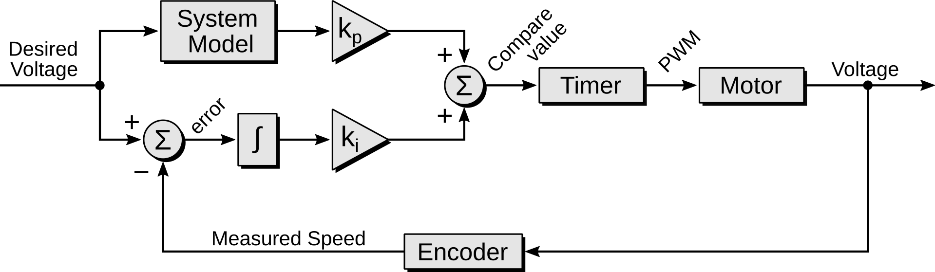
PWM controlled RC circuit
As shown, the proportional control component is an Open-Loop Control, where the generated contribution is dependent only on the value of the desired voltage. The proportional control is supported by a crude system model that attempts to convert a desired voltage into a timer compare value, which is then scaled by the Proportional Gain Constant, \(k_p\). The integral control component is a Closed-Loop Control, with the encoder measurements used to calculate the response error. The response error is integrated (simplified: summed) over time and scaled by the Integral Gain Constant, \(k_i\).
This control scheme is provided in the template project and does not need to be implemented. However, the values for \(k_p\) and \(k_i\) will need to be adjusted to cause the system to operate properly.
12.4. Instructions
12.4.1. Part 1
Import the template project for this activity:
activity_adc14-rc.zip. This project has Timer_A2 preconfigured to generate a PWM output at 1 kHz and has the control algorithm described above written already.Insert the potentiometer into a breadboard and connect two of the legs to ground and 3.3V (see left portion of schematic below). The wiper of the potentiometer, denoted as DESIRED, needs to be connected to a GPIO with analog support, such as P6.1. Pins that have analog support may be identified within the GPIO Alternate Functions table, specifically, by looking at the tertiary column, where analog is denoted by a# (where # is the ADC channel number).

Activity 11 Schematic
Complete the ADC initialization function
ADCInit(). Use the guidance from above and:
Configure the ADC clock to be 6 MHz.
Use the ADC in Single Sample Mode.
Set the microcontroller power supply voltage, 3.3 V, as the reference voltage (AVCC).
The ADC input channel is dependent on the GPIO pin used (e.g., P6.1). The associated channel number may be found in Alternate Functions as noted above.
Within the
if(timer_flag)statement inside themain()functionwhile(1)loop:
add code to trigger the ADC conversion,
wait for the result,
save the result into the variable
uint16_t pot_val,calculate the voltage measured by the ADC (use equation from the lecture or the ADC14 Documentation) and save into the
float desiredvariable. Be careful of integer division here!Note: Printing of the variables is already added.
Connect the USB Test Device or bench-top oscilloscope such that the potentiometer output value is measured. You may alternatively use one of the multimeters in the laboratory for this.
Run and test the code: If working correctly, the printed potentiometer output should match the measurement from the USB Test Device. Rotate or turn the potentiometer to change the output voltage and verify that the printed and measured voltages react accordingly.
12.4.2. Part 2
Build the RC circuit (10 kΩ, 1 μF, \(f_\mathrm{cutoff}\approx 16 \mathrm{Hz}\)) on a breadboard along with the potentiometer (see right portion of schematic above). Note that the left and right portions of the schematic are not physically connected. The PWM will be output from P5.6 and the capacitor voltage, denoted as ACTUAL, connected to a GPIO with analog support, such as P6.0 (ADC input pin).
Modify the ADC initialization function to include conversions on the added pin:
The two conversions should be configured to use adjacent
ADC_MEMxlocations, e.g.,ADC_MEM0andADC_MEM1.Change the ADC to use Multiple Channel Mode (Multi-Sequence Mode).
Add additional lines of code within the
main()function to save the result for the RC circuit output intouint16_t rc_valand calculate the corresponding voltage intofloat actual.Uncomment the “Control Routine” marked within
if(timer_flag){.Connect the USB Test Device oscilloscope, or bench-top oscilloscope, such that both the raw PWM output and capacitor voltage are being monitored. When running, the oscilloscope should show 2-5 cycles of the PWM output.
Run and test the code: The capacitor voltage (
actual) should approach the potentiometer voltage (desired) , albeit very poorly:
The default control constants (
kp = 0.1, ki = 0) are not good. Do not expect the setpoint and capacitor value to match well for this step.Verify that the PWM is being generated via the USB Test Device and the RC filter is working properly.
Rotate the potentiometer to change the desired output value. The PWM duty cycle and capacitor voltage should change, correspondingly.
Refer to the Gradescope assignment for the remainder of the activity. The steps required in the assignment are repeated here:
Submit a screenshot of the oscilloscope showing the PWM and capacitor voltage.
Record the actual voltage output from the RC filter for for when the desired voltage is approximately 0.5 V, 1.5 V, and 2.5 V.
Change the proportional gain constant, kp, from 0.1 to 0.05 and repeat the measurements.
Adjust the integral gain constant, ki, to find a value that causes the target and actual voltage to match reasonably well. For initial testing, have the actual voltage be approximately 1.5 V. Once a good value is found, ensure that the value works for other values of the target voltage. Record the working value for ki.
Reset kp back to 0.1, leaving ki with the value found above. Describe how the system response changes (qualitatively) with this higher kp.
Increase ki until the system no longer behaves well. What went wrong with the system response?
Submit your final code.