|
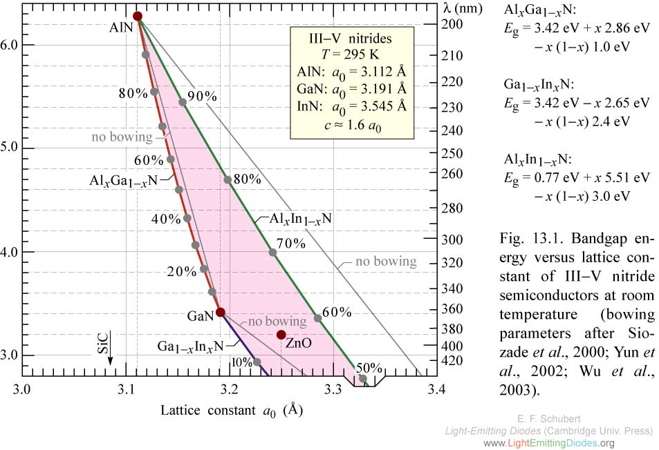
Fig. 13.1. Bandgap energy versus lattice constant of III-V nitride semiconductors at room temperature (bowing parameters after Siozade et al., 2000; Yun et al., 2002; Wu et al., 2003).
|
|
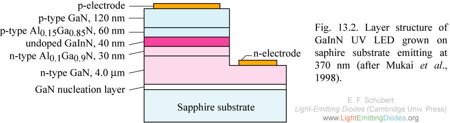
Fig. 13.2. Layer structure of GaInN UV LED grown on saphire substrate emitting at 370 nm (after Mukai et al., 1998).
|
|
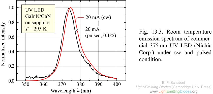
Fig. 13.3. Room temperature emission spectrum of commercial 375nm UV LED (Nichia Corp.) under cw and pulsed condition.
|
.jpg)
|
Fig. 13.4. Room temperature emission intensity as a function of GaInN active layer thickness for double heterostructure UV LEDs emitting at 375nm (after Mukai et al., 1998).
|
|
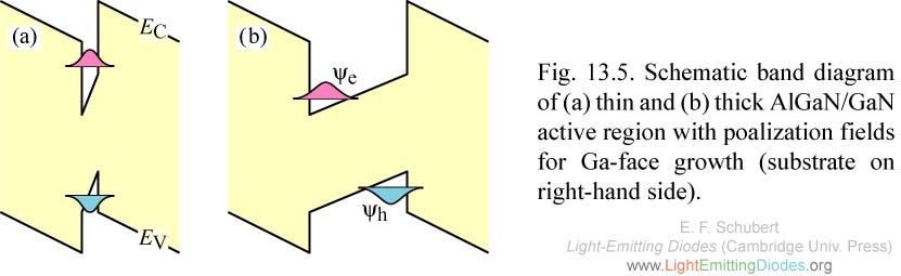
Fig. 13.5. Schematic band diagram of (a) thin and (b) thick AlGaN/GaN active region with poalization fields for Ga-face growth (substrate on right-hand side).
|
.jpg)
|
Fig. 13.6. Room temperature intensity as a function of emission wavelength for GaInN double heterostructure UV LEDs (after Mukai et al., 1998).
|