|
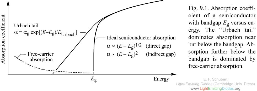
Fig. 9.1. Absorption coefficient of a semiconductor with bandgap Eg versus energy. The “Urbach tail” dominates absorption near but below the bandgap. Absorption further below the bandgap is dominated by free-carrier absorption.
|

|
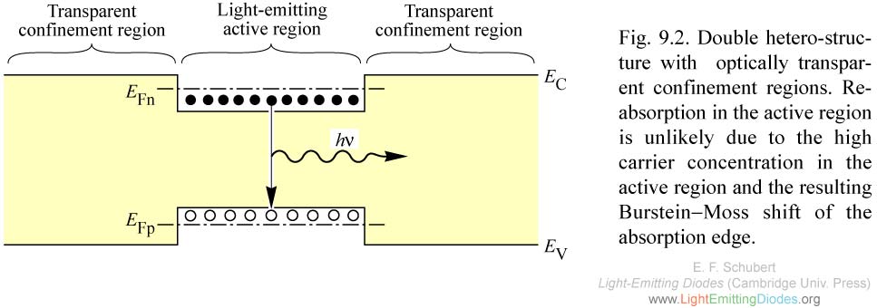
Fig. 9.2. Double hetero-structure with optically transparent confinement regions. Reabsorption in the active region is unlikely due to the high carrier concentration in the active region and the resulting Burstein-Moss shift of the absorption edge.
|

|
Fig. 9.3. “Trapped light” in a rectangular-parallelepiped-shaped semiconductor unable to escape for emission angles greater than alpha c due to total internal reflection.
|

|
Fig. 9.4. Schematic illustration of different geometric shapes for LEDs with perfect extraction efficiency. (a) Spherical LED with a point-like light-emitting region at the center of the sphere. (b) A cone-shaped LED.
|

|
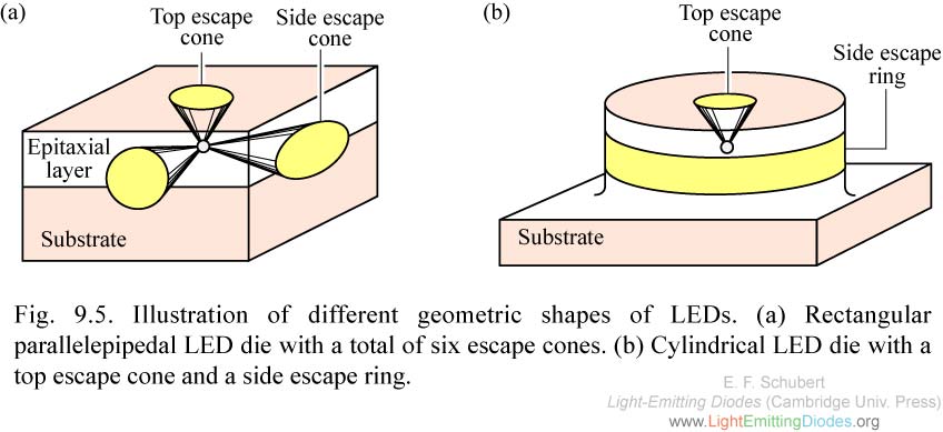
Fig. 9.5. Illustration of different geometric shapes of LEDs. (a) Rectangular parallelepipedal LED die with a total of six escape cones. (b) Cylindrical LED die with a top escape cone and a side escape ring.
|

|
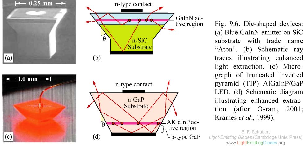
Fig. 9.6. Die-shaped devices: (a) Blue GaInN emitter on SiC substrate with trade name “Aton”. (b) Schematic ray traces illustrating enhanced light extraction. (c) Micrograph of truncated inverted pyramid (TIP) AlGaInP/GaP LED. (d) Schematic diagram illustrating enhanced extraction (after Osram, 2001; Krames et al., 1999).
|

|
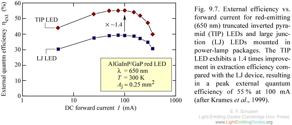
Fig. 9.7. External efficiency vs. forward current for red-emitting (650 nm) truncated inverted pyramid (TIP) LEDs and large junction (LJ) LEDs mounted in power-lamp packages.
|

|
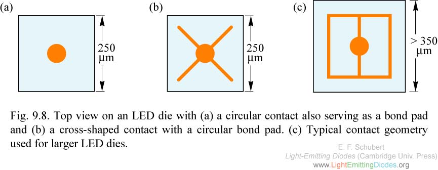
Fig. 9.8. Top view on an LED die with (a) a circular contact also serving as a bond pad and (b) a cross-shaped contact with a circular bond pad. (c) Typical contact geometry used for larger LED dies.
|

|
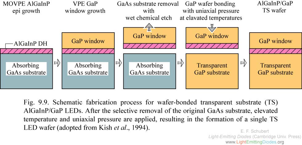
Fig. 9.9. Schematic fabrication process for wafer-bonded transparent substrate (TS) AlGaInP/GaP LEDs. After the selective removal of the original GaAs substrate, elevated temperature and uniaxial pressure are applied, resulting in the formation of a single TS LED wafer (adopted from Kish et al., 1994).
|

|
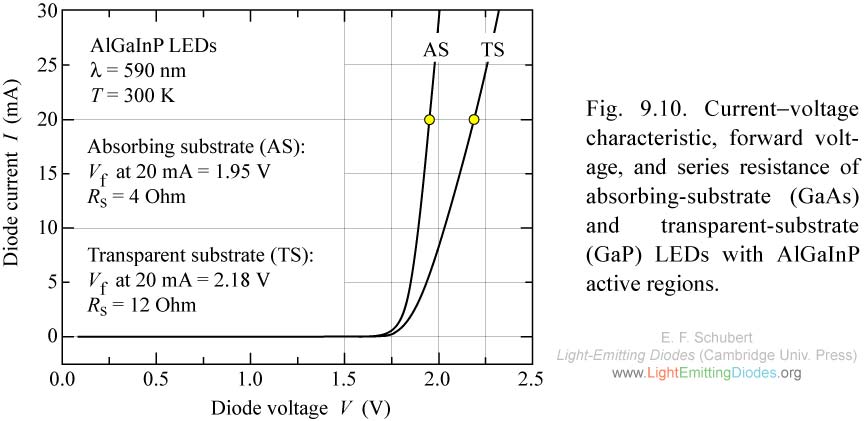
Fig. 9.10. Current-voltage characteristic, forward voltage, and series resistance of absorbing-substrate (GaAs) and transparent-substrate (GaP) LEDs with AlGaInP active regions.
|

|
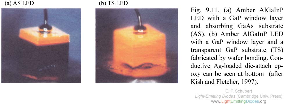
Fig. 9.11. (a) Amber AlGaInP LED with a GaP window layer and absorbing GaAs substrate (AS). (b) Amber AlGaInP LED with a GaP window layer and a transparent GaP substrate (TS) fabricated by wafer bonding. Conductive Ag-loaded die-attach epoxy can be seen at bottom (after Kish and Fletcher, 1997).
|

|
Fig. 9.12. Illustration of optimum thickness and refractive index of an anti-reflection (AR) coating. |
